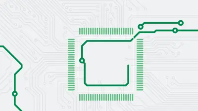
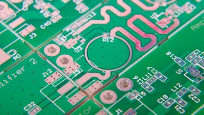
Radio frequency (RF) printed circuit boards (RF PCBs)
Radio frequency (RF) printed circuit boards (PCBs) are highly specialized RF boards engineered to reliably operate at high radio frequencies from tens of megahertz up to tens of gigahertz for wireless communications applications. With precision impedance control and low-loss materials, RF PCBs can effectively route and radiate RF signals with minimal interference, loss, or distortion, even at microwave frequency ranges.
What are RF printed circuit boards?
An RF circuit board is an analog printed circuit board designed using proprietary materials, layer stackups, and layout techniques to facilitate processing and efficient transmission of wireless signals modulated onto a high-frequency carrier wave.
Key characteristics of RF PCB technology:
- Engineered for radio frequency operation from 30 MHz up to 50 GHz and beyond
- Carry modulated wireless communication and radar signals along with lower frequency control data
- Incorporate microstrip or stripline transmission lines with tightly controlled characteristic impedance, typically 50 or 75 ohm
- Maintain signal integrity and purity with minimal attenuation at multi-gigahertz frequencies
- Utilize advanced PCB substrate materials with low loss tangent and stable dielectric properties over the RF spectrum
- Allow for the integration of active components like MMICs and passive components like filters/attenuators
- Implement shielding structures such as ground planes and guard traces to reduce crosstalk
RF PCBs enable wireless transmission and reception of information content modulated onto a high-frequency sine-wave carrier signal. This facilitates networking and control between electronic devices and systems that need to wirelessly transfer data and signals through the air interface for radio communications, radar, navigation, IoT, automation, and other wireless connectivity applications.
A specialty in this segment are RF PCBs specifically designed to function at microwave frequencies (i.e., tens of gigahertz and beyond). They are characterized by precision impedance control and high-grade, low-loss materials. This dynamic duo ensures that RF signals are routed and radiated with pinpoint accuracy, minimizing loss, interference, and distortion. Perfect for applications ranging from high-speed data transmission to cutting-edge radar technology, Microwave PCBs deliver unparalleled performance across a broad spectrum of wireless needs.
Key features include controlled impedance typically around 50 or 75 ohm, advanced substrate materials with a low loss tangent, and design flexibility that allows for seamless integration of active and passive components. These boards also boast shielding structures like ground planes and guard traces, effectively reducing crosstalk and ensuring signal integrity.
Why use RF printed circuit board technology?
There are several key advantages of using radio frequency PCBs instead of conventional PCBs for high-frequency analog and digital signal applications:
Wireless connectivity
RF PCBs readily facilitate wireless communication between devices over various standards like Bluetooth, WiFi, ZigBee, RFID, cellular, LoRa, and more.
Wide frequency range
They cover hundreds of MHz to tens of GHz, supporting the majority of wireless bands for modern communications, radar, broadcasting, navigation, and telemetry applications.
Controlled impedance
Precision 50- or 75-ohm impedance-matched transmission lines prevent reflections and maximize power transfer efficiency and range.
Signal integrity
Stable electrical performance results in distortion-free wave propagation with minimal attenuation or interference at GHz frequencies.
Miniaturization
High-density RF circuits can be fully integrated into the PCB layout, eliminating extra wiring. This allows for substantial size reduction of end products.
Reliable performance
Robust electrical design, controlled impedance mismatches, and advanced materials provide dependable functionality under demanding high-frequency operating conditions.
Design flexibility
RF PCBs support the integration of both analog and digital signals on the same RF PCB for mixed-signal designs. Less wiring means fewer potential points of failure.
Simulation and modeling
Used to model RF circuits with suitable material properties and to run electromagnetic field simulations to verify high-frequency operation prior to fabrication. Reduces guesswork and re-spins.
RF PCB design guidelines and design process of RF boards
Successfully designing and implementing RF circuit boards demands special attention to impedance control, transmission line effects, isolation, shielding, and more at GHz frequencies. Proper RF PCB layout technique is crucial to achieve the design objectives of precise impedance control, low loss, distortion-free wave propagation and immunity to interference at the intended operating radio frequencies.
Controlled impedance lines
Use of impedance matching techniques to maintain 50 or 75 ohm transmission-line impedance based on width/height ratios.
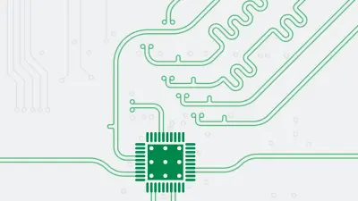
RF transmission lines
Use of microstrip, stripline, or coplanar types. Avoids stubs, length changes, and 90-degree bends that cause reflections.
Layer stack and sequence
Strategic placement of ground and power planes to sandwich signal layers for shielding and isolation.
RF component placement
Grouping and orienting components according to function. RF components get placed first near controlled impedance lines.
Routing
Route traces that are as straight as possible point-to-point. Use of 45-degree bends, avoiding 90-degree turns. Equalization of line lengths.
Shielding and isolation
Employing ground planes, guard bands, shielding enclosures, and distance separation between RF and noisy digital circuits.
Bypassing and decoupling
Use of dedicated RF bypass/decoupling capacitors at each IC power pin located near RF signal traces.
Simulation
Modelling of layouts with suitable material properties and stackups. Running of EM simulations to verify performance before fabrication.
Common RF PCB substrate materials
Since standard FR-4 material lacks adequate performance at high frequencies, radio frequency PCBs require specialized substrate materials engineered to provide:
- Tight impedance tolerances over the RF spectrum
- Low loss tangent resulting in minimal signal attenuation
- Stable dielectric constant (Dk) over the operating frequency range
- Consistent performance over the operating temperature range
- Moisture absorption limits
- Strong thermal performance
PTFE ceramic filled: Extremely low loss and highly stable Dk extending above 10 GHz. Often used for stripline implementations.
Woven-glass-reinforced PTFE: Lower moisture absorption properties. Excellent thermal stability. Well suited for microstrip circuits.
Modified epoxy blends: Cost effective RF material with good performance up to 6 GHz wireless bands making it suitable for WiFi/BLE.
Hydrocarbon ceramic blends: Stable properties at very high frequencies up to 77 GHz and beyond for emerging mmWave applications.
PTFE-ceramic composites: Exotic low-loss materials usable over 100 GHz with tight impedance control required in specialized equipment.
Rigid or Flex Laminates: Many RF materials are available on both rigid laminates as well as flex circuit substrates.
Material selection involves tradeoffs between cost, electrical and thermal performance, and manufacturability based on the target application requirements.


Partner with copperdot for your next RF PCB project
With extensive capabilities to deliver an array of PCB types, copperdot can provide specialized RF PCB fabrication services tailored to your design requirements, including operating frequency, layer count, materials, target impedance, and electrical performance.
Our RF PCB manufacturing capabilities include:
- FR-4 dielectric material for cost-effective lower-frequency boards
- Wide range of RF materials including ceramic PTFE composites, hydrocarbon ceramics, epoxy blends
- Layer counts from 4-layer to >12-layer designs
- Tight impedance control and tolerances
- Skilled layout expertise for optimal RF performance
- Quick turn prototyping services
- Medium-volume production capacity
To get an instant RFQ or discuss your next project’s needs in greater detail, simply upload your Gerber design files or contact us. Our engineering team will ensure your design gets manufactured as a high-performance radio frequency PCB tailored to your wireless application requirements.
Frequently asked questions about RF PCBs
RF PCBs use tightly controlled impedance lines and low-loss dielectric materials to maintain signal integrity at multi-gigahertz frequencies. Digital PCBs use standard FR4 and focus primarily on high-speed digital data transmission.
Controlled impedance transmission lines, strategic layer stacks, isolation structures, minimized trace lengths, and bypassing IC power pins are essential for clean RF signal propagation with minimal reflections, leakage, or losses.
Specialized low-loss microwave substrate materials like PTFE composites with a stable dielectric constant are used along with precise fabrication processes to enable functionality up to 100 GHz.
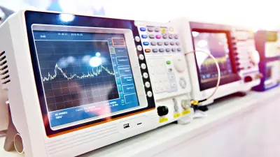
In addition to standard inspection and netlist testing, RF PCBs require extensive high-frequency electrical testing like impedance, insertion loss, VSWR, and isolation measurements on coupons and/or finished boards.