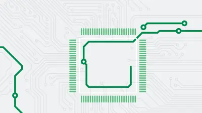
What Are HDI (High-Density Interconnect) PCBs?
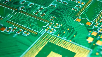
High-density interconnect (HDI) PCBs are advanced printed circuit boards that enable higher component density and provide more routing channels than traditional circuit boards. HDI technology makes it possible to pack more components into a given area by utilizing very fine lines and spaces between copper traces.
Understanding HDI PCBs
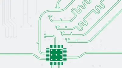
A high-density interconnect (HDI) PCB is a type of printed circuit board fabricated using specialized materials and advanced manufacturing processes to achieve much finer traces, smaller vias, higher component density, and more layers compared to standard PCBs.
HDI PCBs incorporate the latest innovations in PCB technology to enable greater wiring density and component density on the board by utilizing thinner dielectric insulating materials between layers and finer track widths and spacing between copper traces. They employ tiny microvias with smaller drill diameters to interconnect the traces between layers. This maximizes routing area utilization and provides more design flexibility.
Some of the key features and capabilities of high-density interconnect PCBs are:
- High layer counts — 10 layers or more
- Very fine track widths and trace spacing — widths as low as 3 mil or 4 mil are common
- Higher-density component layouts
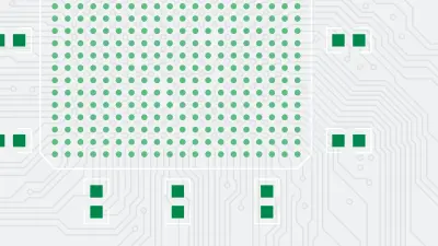
- Microvias with smaller drill diameters, usually 0.15 mm (150 microns) or less
- Thinner dielectric insulating material layers, with a typical thickness of 3 mil or 4 microns thickness or less
- Fabricated using a sequential lamination process
- High wiring density per unit area
- Facilitates the routing of densely packed BGA, CSP, and other fine-pitch components
Benefits of using HDI PCBs
Compared to conventional PCBs, HDI PCB technology provides designers and engineers with the following advantages:
Achieve greater component density
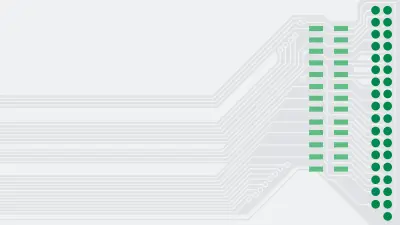
The fine line widths and trace spacings achieved in HDI PCBs allow for components to be placed very close together in a dense layout, enabling smaller and lighter end products.
Increase routing density
The high-density interconnects facilitate more routing channels per layer, which increases overall wiring capacity for laying out complex and dense board designs.
Enable miniaturization of electronics
By packing more functionality into a compact PCB area, HDI technology facilitates miniaturization and weight reduction of end products such as mobile devices.
Improves electrical performance
The smaller microvias, tighter trace spacing, and thinner dielectric materials in HDI boards enhance signal speed through closely spaced traces and minimize interference or crosstalk, improving signal integrity.
Gain more design flexibility
The high-density interlayer connections provided by laser-drilled microvias facilitate routing paths for densely packed components with high pin counts, such as BGA packages.
Reduce PCB layer count
Since the available routing area per layer is utilized very efficiently, HDI board designs can potentially achieve the same circuit connectivity and component placement with fewer PCB layers compared to conventional designs. This helps lower fabrication costs.
Types of HDI PCB stack-ups
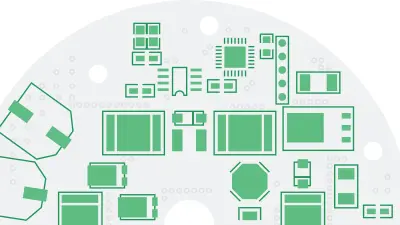
The areas of application for rigid printed circuit boards in electronic devices are many and varied. The used in almost all areas of life and are standard when it comes to electronic controls and circuits:
1+N+1 HDI: This stackup has one signal routing layer on the top layer and one signal layer on the bottom layer. In between are N number of sequentially laminated buildup layers comprised of alternating dielectric and copper layers, where N can typically range from four to more than 8.
2+N+2 HDI: This configuration has two outer signal layers — top and bottom — sandwiching N number of sequential buildup layers in the middle. Provides routing on four outer layers.
3+N+3 HDI: As the name indicates, this type has three signal layers on the outer top, middle, and bottom of the stackup with N number of sequential buildup layers in between. Provides routing on six outer layers.
Any Layer HDI: This is the most advanced type, where high-density interconnects are provided on any or all layers including the core layers. Maximizes routing flexibility.
The 1+N+1 and 2+N+2 designs are the most common, while 3+N+3 and Any Layer provide more complex and higher-performance interconnect solutions. The buildup layers use very thin dielectrics and dense microvias.
How HDI PCBs are manufactured
To fabricate a high-quality HDI printed circuit board, PCB manufacturers use specialized materials and advanced manufacturing processes:
Laser drilling for microvias
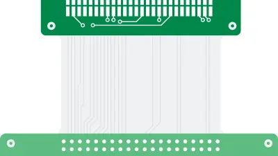
Microvias in HDI boards are most commonly laser-drilled to achieve the small via diameters of around 50 microns (0.005 cm) or less along with highly precise hole location. Laser drilling can also be used for staggered and stacked microvias for optimal routing.
Using ultra-thin dielectric materials
A very thin base dielectric material of 1 mil (0.001") or 25 microns is used for core layers. Sequential buildup layers are also fabricated using thin dielectric laminates. This makes it possible to achieve fine trace geometries in terms of line width and line spacing.
Sequential lamination process
Unlike standard lamination cycles, in sequential lamination, the core and buildup dielectric materials along with copper foils are laminated one layer at a time. This achieves overall board thicknesses as low as 0.4 mm for a 10+ layer count HDI board.
Copper plating for microvias
The microvia holes are plated with copper using electroless and electrolytic plating processes to create a continuous conductive pathway between the layers interconnected by the via.
Precision routing and laser imaging
Very fine line patterns are achieved during the routing and imaging process thanks to tight tolerance laser imaging. The sequential buildup process minimizes registration issues for greater precision.
Comprehensive electrical testing
Each completed HDI PCB undergoes 100% electrical testing using flying probe or bed of nails testers. This verifies the reliability of the high-density microvia interconnections between layers.


Why choose copperdot for your HDI PCB solutions?
copperdot is the new global hub for PCB procurement. We are disrupting the old, complex, and slow way of sourcing PCBs that everyone is used to. copperdot will orchestrate the entire HDI PCB production process on your behalf, allowing you to concentrate on product development. We can collaborate to optimize an HDI design or match finished designs with manufacturers based on their expertise. All you need to do is look forward to receiving your high quality HDI PCBs on time, confident they will perform as expected.
Our HDI PCB capabilities include:
- High layer count designs — six layers and above
- Line width and line spacing down to 2 mil
- Microvias with 5 mil diameters drilled with precision lasers
- Utilization of 1 mil thin core dielectric layers
- Cycle time optimization through engineering collaboration
- 100% bare board electrical testing of every HDI board
- Quick turn engineering prototypes with fast iterations
- Medium- and low-volume production — up to 1,000 pieces
To get an instant free HDI PCB quote or discuss your next HDI project in greater detail, simply use our online inquiry form or contact us via e-mail or by phone. Our team of engineers is ready to partner with you and deliver advanced interconnect solutions for your complex designs using cutting-edge HDI technology tailored to your requirements.
HDI PCB FAQs
HDI PCBs allow for much higher routing density and component density compared to conventional PCBs by utilizing thinner dielectric layers, smaller microvias, finer trace geometries, and higher layer counts in the range of eight layers or more.
Microvias are very small vias, typically with a diameter of less than 150 microns (0.15 mm) that are used to interconnect traces between layers on HDI PCBs. Microvias are most commonly laser drilled and then plated with copper to create a conductive path between layers.
Some popular HDI layer stackups are 1+N+1, 2+N+2, and 3+N+3 configurations, which have N number of sequential buildup layers between outer signal routing layers. Any Layer HDI allow for interconnects on any layer.
Yes, plated through-hole components can be accommodated on HDI PCBs by providing clearance holes in the high-density buildup layers so that the barrels of the holes pass through unobstructed.