Understanding HDI PCBs: the future of compact and efficient circuit design

HDI (High-Density-Interconnect) PCBs are at the forefront of modern circuit board technology. With the ongoing miniaturization of devices across industries, HDI PCBs have become pivotal when it comes to meeting the complex requirements of today’s compact electronic gadgets.
What are HDI PCBs?
HDI PCBs are printed circuit boards with a higher wiring density per unit area than traditional PCBs. They utilize finer lines and spaces, smaller vias and capture pads, and higher connection pad densities. An High-Density-Interconnect PCB typically incorporates microvias, which are tiny holes drilled by a laser that can be as small as 0.003–0.006 inches (0.076–0.15 mm) in diameter.

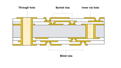
These microvias allow for connections between layers without the need for larger through-holes, enabling higher component density. There are two types of microvias: buried vias (connecting inner layers) and blind vias (connecting outer and inner layers) that route connections, further increasing circuit density.
The lines and spaces on an HDI PCB can be as fine as 0.003 inches (0.076 mm), compared to 0.006 inches (0.152 mm) for standard PCBs. Combined with the use of microvias, this finer trace geometry allows HDI PCBs to fit up to 60% more components in the same area as a conventional PCB.
HDI PCBs are typically manufactured using a sequential lamination process where thin laminates are built up layer by layer and coupled with laser-drilled microvias to form the dense interconnect structure.
Specialized manufacturing process of HDI PCBs
The manufacturing of HDI PCBs involves several advanced techniques that set them apart from conventional PCBs:
Sequential lamination: Multiple layers of thin materials are laminated together in sequences to build up the PCB. This process allows for the inclusion of microvias, buried vias, and through vias that connect the various layers of the board.
Laser drilling: Used to create microvias, laser drilling provides the high level of precision needed to produce the small and complex vias required in HDI boards.
The benefits of using High-Density-Interconnect PCBs are significant. HDI PCBs allow for a more compact device footprint and they can offer improved electrical performance and enable faster transmission speeds. Additionally, they can support more input/output in smaller geometries. This reduction in size does not come at the expense of performance, which makes these PCBs highly sought-after in advanced technological applications.
Despite their many benefits, HDI PCBs come with challenges. The primary disadvantage is cost; HDI PCBs are generally more expensive to produce than traditional PCBs due to the specialized materials and processes involved, such as laser drilling, sequential lamination, and other HDI processes that require specialized equipment and expertise, driving up manufacturing costs. Moreover, the intricate nature of HDI designs demands more engineering hours, costly prototyping cycles, and stringent quality control measures – all adding to the overall expense.
Design considerations for HDI PCBs
Designing High-Density-Interconnect HDI PCBs requires careful planning and adherence to best practices to ensure signal integrity, thermal performance, and manufacturability. Key design considerations include:
Signal integrity: The tighter spacing in HDI PCBs increases susceptibility to crosstalk, impedance discontinuities, and other signal degradation issues. Thorough signal integrity analysis and simulations are crucial.
Thermal management: The high component density of HDI PCBs can lead to heat dissipation challenges. Thermal modeling, via sizing, and dedicated thermal zones must be implemented.
CAD tools: HDI design requires advanced CAD tools capable of handling dense data sets, microvias, buried vias, and other HDI features.
Design for manufacturing (DFM): Close collaboration with the manufacturer’s or supplier’s DFM team is critical. DFM reviews catch potential issues early on, optimizing the design for cost-effective and reliable HDI fabrication.
Why copperdot is the right service for HDI PCB procurement
At Bosch, copperdot specializes in delivering high-quality HDI PCBs tailored to your specific needs. By choosing copperdot, you benefit from:
Expert guidance
Our team provides expertise in navigating the complexities of HDI PCB design and production. We apply DFM principles to optimize your HDI PCB designs for cost-effectiveness and manufacturability.
Quality assurance
We ensure that each PCB meets the highest standards in terms of quality and reliability.
Cost-effectiveness
Despite the inherent costs of HDI technology, copperdot strives to provide cost-effective solutions without compromising on quality.
Extensive supplier network
Leverage our tested and trusted network of PCB manufacturers to find the ideal supplier for your project requirements.
Material expertise
Benefit from Bosch’s extensive knowledge of materials to ensure your PCBs use the most effective and compliant resources.
Efficient logistics
Our streamlined logistics ensure smooth and timely delivery of your PCBs.
Conclusion
For industry decision-makers who rely on advanced electronic components, understanding the benefits and challenges of HDI PCBs is crucial. As devices become increasingly integrated, the demand for sophisticated solutions like HDI PCBs will only grow. With copperdot, you gain a partner committed to delivering superior results. Choose copperdot for your HDI PCB needs and join us in shaping the future of electronic product design.


