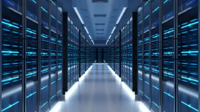
Back panel PCBs: the control centers of modern electronics
What are back panel PCBs?
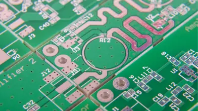
Material matters: the base materials of back panel PCBs
Choosing the right materials affects the performance and longevity of a back panel PCB. Commonly used materials include:
- FR4 (Flame Retardant 4): standard material with good electrical and mechanical properties
- PTFE (Polytetrafluoroethylene): high frequency material with low dielectric constant
- Metal core PCBs: increased heat dissipation for high-performance applications. The choice of suitable material depends on factors such as operating temperature, signal speed and mechanical stability with mid or high Tg.
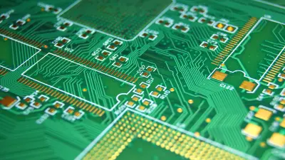
Surface advantages: why surface quality matters in PCB performance
The surface finish of a back panel PCB has a direct influence on its performance. Important aspects are:
Solder resist masks
protect copper structures from oxidation and improve solderability
Gold or silver surfaces
ensure low contact resistance and increased service life
Planar surfaces
reduce signal loss and electromagnetic interference. The quality of the surface influences both the electrical performance and the mechanical reliability of a back panel PCB.
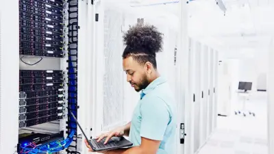
Integrating back panel PCBs: enhancing system efficiency and reliability
Back panel PCBs contribute to the optimization of systems by:
- Reducing the amount of cable: fewer physical connections mean higher reliability.
- Improving signal integrity: reducing signal loss through optimized traces.
- Supporting thermal management: specialized materials and designs help prevent overheating. Through precise planning and integration, back panel PCBs can significantly increase the efficiency and longevity of electronic systems.
Future trends: innovations in back panel PCB design and manufacturing
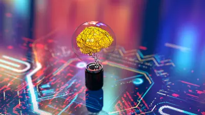
The future of back panel PCBs will be shaped by new technologies and materials. Key developments include high-frequency PCBs, optimized for 5G and IoT applications, as well as flexible and rigid-flexible back panel designs that allow for space-saving and robust structures. Additionally, automated manufacturing techniques, supported by AI, enable more efficient production. These innovations make back panel PCBs more powerful and reliable, meeting the increasing demands of modern electronics.
System performance starts with the details.